- 您现在的位置:买卖IC网 > Sheet目录342 > MCBSTM32EXL (Keil)BOARD EVALUATION FOR STM32F103ZE
�� �
�
�Backup� registers� (BKP)�
�RM0008�
�5.4�
�5.4.1�
�BKP� registers�
�Refer� to� Section� 1.1� on� page� 37� for� a� list� of� abbreviations� used� in� register� descriptions.�
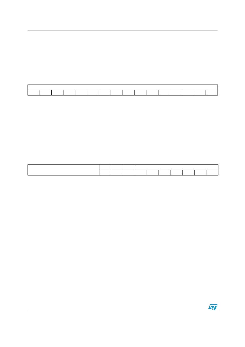
�Backup� data� register� x� (BKP_DRx)� (x� =� 1� ..42)�
�Address� offset:� 0x04� to� 0x28,� 0x40� to� 0xBC�
�Reset� value:� 0x0000� 0000�
�15�
�14�
�13�
�12�
�11�
�10�
�9�
�8�
�7�
�6�
�5�
�4�
�3�
�2�
�1�
�0�
�D[15:0]�
�rw�
�rw�
�rw�
�rw�
�rw�
�rw�
�rw�
�rw�
�rw�
�rw�
�rw�
�rw�
�rw�
�rw�
�rw�
�rw�
�Bits� 15:0� D[15:0]� Backup� data�
�These� bits� can� be� written� with� user� data.�
�Note:� The� BKP_DRx� registers� are� not� reset� by� a� System� reset� or� Power� reset� or� when� the�
�device� wakes� up� from� Standby� mode.�
�They� are� reset� by� a� Backup� Domain� reset� or� by� a� TAMPER� pin� event� (if� the� TAMPER�
�pin� function� is� activated).�
�5.4.2�
�RTC� clock� calibration� register� (BKP_RTCCR)�
�Address� offset:� 0x2C�
�Reset� value:� 0x0000� 0000�
�15�
�14�
�13�
�12�
�11�
�10�
�9�
�8�
�7�
�6�
�5�
�4�
�3�
�2�
�1�
�0�
�ASOS�
�ASOE�
�CCO�
�CAL[6:0]�
�Reserved�
�rw�
�rw�
�rw�
�rw�
�rw�
�rw�
�rw�
�rw�
�rw�
�rw�
�Bits� 15:10� Reserved,� always� read� as� 0.�
�Bit� 9� ASOS:� Alarm� or� second� output� selection�
�When� the� ASOE� bit� is� set,� the� ASOS� bit� can� be� used� to� select� whether� the� signal� output� on�
�the� TAMPER� pin� is� the� RTC� Second� pulse� signal� or� the� Alarm� pulse� signal:�
�0:� RTC� Alarm� pulse� output� selected�
�1:� RTC� Second� pulse� output� selected�
�Note:� This� bit� is� reset� only� by� a� Backup� domain� reset.�
�Bit� 8� ASOE:� Alarm� or� second� output� enable�
�Setting� this� bit� outputs� either� the� RTC� Alarm� pulse� signal� or� the� Second� pulse� signal� on� the�
�TAMPER� pin� depending� on� the� ASOS� bit.�
�The� output� pulse� duration� is� one� RTC� clock� period.� The� TAMPER� pin� must� not� be� enabled�
�while� the� ASOE� bit� is� set.�
�Note:� This� bit� is� reset� only� by� a� Backup� domain� reset.�
�Bit� 7� CCO:� Calibration� clock� output�
�0:� No� effect�
�1:� Setting� this� bit� outputs� the� RTC� clock� with� a� frequency� divided� by� 64� on� the� TAMPER� pin.�
�The� TAMPER� pin� must� not� be� enabled� while� the� CCO� bit� is� set� in� order� to� avoid� unwanted�
�Tamper� detection.�
�Note:� This� bit� is� reset� when� the� V� DD� supply� is� powered� off.�
�68/995�
�Doc� ID� 13902� Rev� 9�
�发布紧急采购,3分钟左右您将得到回复。
相关PDF资料
MCBTMPM330
BOARD EVAL TOSHIBA TMPM330 SER
MCIMX25WPDKJ
KIT DEVELOPMENT WINCE IMX25
MCIMX53-START-R
KIT DEVELOPMENT I.MX53
MCM69C432TQ20
IC CAM 1MB 50MHZ 100LQFP
MCP1401T-E/OT
IC MOSFET DRVR INV 500MA SOT23-5
MCP1403T-E/MF
IC MOSFET DRIVER 4.5A DUAL 8DFN
MCP1406-E/SN
IC MOSFET DVR 6A 8SOIC
MCP14628T-E/MF
IC MOSFET DVR 2A SYNC BUCK 8-DFN
相关代理商/技术参数
MCBSTM32EXLU
功能描述:开发板和工具包 - ARM EVAL BOARD + ULINK2 FOR STM32F103ZG
RoHS:否 制造商:Arduino 产品:Development Boards 工具用于评估:ATSAM3X8EA-AU 核心:ARM Cortex M3 接口类型:DAC, ICSP, JTAG, UART, USB 工作电源电压:3.3 V
MCBSTM32EXLU-ED
制造商:ARM Ltd 功能描述:KEIL STM STM32EXL EVAL BOARD
MCBSTM32EXLUME
功能描述:开发板和工具包 - ARM EVAL BOARD + ULINKME FOR STM32F103ZG
RoHS:否 制造商:Arduino 产品:Development Boards 工具用于评估:ATSAM3X8EA-AU 核心:ARM Cortex M3 接口类型:DAC, ICSP, JTAG, UART, USB 工作电源电压:3.3 V
MCBSTM32F200
功能描述:开发板和工具包 - ARM EVAL BOARD FOR STM STM32F207IG
RoHS:否 制造商:Arduino 产品:Development Boards 工具用于评估:ATSAM3X8EA-AU 核心:ARM Cortex M3 接口类型:DAC, ICSP, JTAG, UART, USB 工作电源电压:3.3 V
MCBSTM32F200U
功能描述:开发板和工具包 - ARM EVAL BOARD FOR STM STM32F207IG + ULINK2
RoHS:否 制造商:Arduino 产品:Development Boards 工具用于评估:ATSAM3X8EA-AU 核心:ARM Cortex M3 接口类型:DAC, ICSP, JTAG, UART, USB 工作电源电压:3.3 V
MCBSTM32F200UME
功能描述:开发板和工具包 - ARM EVAL BOARD FOR STM STM32F207IG ULINK-ME
RoHS:否 制造商:Arduino 产品:Development Boards 工具用于评估:ATSAM3X8EA-AU 核心:ARM Cortex M3 接口类型:DAC, ICSP, JTAG, UART, USB 工作电源电压:3.3 V
MCBSTM32F200UME-ED
制造商:ARM Ltd 功能描述:KEIL STM32F207IG EVAL BOARD
MCBSTM32F400
功能描述:开发板和工具包 - ARM EVAL BOARD FOR STM STM32F407IG
RoHS:否 制造商:Arduino 产品:Development Boards 工具用于评估:ATSAM3X8EA-AU 核心:ARM Cortex M3 接口类型:DAC, ICSP, JTAG, UART, USB 工作电源电压:3.3 V